作者:ADI公司 George Diniz,产品线经理
Abstract
摘要
The JESD204A/JESD204B industry standard for serial interfaces was developed to address the problem of interconnecting the newest wideband data converters with other system ICs in an efficient and cost saving manner. The motivation was to standardize an interface that would reduce the number of digital inputs/outputs between data converters and other devices, such as field programmable gate arrays (FGPAs) and system on a chip (SoC) devices through the use of a scalable high speed serial interface.
开发串行接口业界标准JESD204A/JESD204B的目的在于解决以高效省钱的方式互连最新宽带数据转换器与其他系统IC的问题。其动机在于通过采用可调整高速串行接口,对接口进行标准化,降低数据转换器与其他器件(如现场可编程门阵列FPGA和系统级芯片SoC)之间的数字输入/输出数量。
Trends show that new applications, as well as advances in existing ones, are driving the need for wideband data converters with increasingly higher sampling frequencies and data resolutions. Transmitting data to and from these wideband converters poses a significant design problem as bandwidth limitations of existing I/O technologies force the need for higher pin counts on converter products. Consequently, systems’ PCB designs have become increasingly more complex in terms of interconnect density. The challenge is routing a large number of high speed digital signals while managing electrical noise. The ability to offer wideband data converters with GSPS sampling frequencies, using fewer interconnects, simplifies the PCB layout challenges, and allows for smaller form factor realization without impacting overall system performance.
趋势显示最新应用,以及现有应用的升级,正不断需求采样频率和数据分辨率更高的宽带数据转换器。向这些宽带转换器传送和获取数据暴露了一个非常大的设计问题,即现有I/O技术带宽的限制导致转换器产品需要使用的引脚数更多。其结果便是PCB设计随着互连密度的增加而更复杂。其挑战在于进行大量高速数据信号走线的同时控制电噪声,以及提供GSPS级别的宽带数据转换器采样频率的能力、使用更少的互连、简化PCB布局难题并实现更小的尺寸,且不降低整体系统性能。
Market forces continue to press for more features, functionality, and performance in a given system, driving the need for higher data-handling capacity. The high speed analog-to-digital converter and digital-to-analog converter-to-FPGA interface had become a limiting factor in the ability of some system OEMs to meet their next generation data-intensive demands. The JESD204B serial interface specification was specifically created to help solve this problem by addressing this critical data link. Figure 1 shows typical high speed converter-to-FPGA interconnect configurations using JESD204A/JESD204B.
市场力量继续施压,要求给定系统拥有更多特性和功能以及更好的性能,推动了对更高数据处理能力的要求。高速模数转换器和数模转换器至FPGA接口已成为某些系统OEM厂商满足下一代大量数据处理需要的限制因素。JESD204B串行接口规范专为解决这一关键数据链路的问题而建立。图1显示使用JESD204A/JESD204B的典型高速转换器至FPGA互连配置。
Some key end-system applications that are driving the deployment of this specification, as well as a contrast between serial low voltage differential signaling (LVDS) and JESD204B, are the subject of the remainder of the article.
本文余下篇幅将探讨推动该规范发展的某些关键的终端系统应用,以及串行低压差分信号(LVDS)和JESD204B的对比。
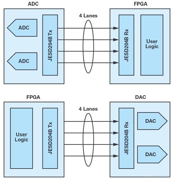
Figure 1. Typical high speed converter to FGPA interconnect configurations using JESD204A/JESD204B interfacing (Source: Xilinx®).
图1.使用JESD204A/JESD204B接口的典型高速转换器至FGPA互连配置(来源:Xilinx®)。
The Applications Driving the Need for JESD204B
应用推动对JESD204B的需求
Wireless Infrastructure Transceivers
无线基础设施收发器
OFDM-based technologies, such as LTE, used in today’s wireless infrastructure transceivers use DSP blocks implemented on FPGAs or SoC devices driving antenna array elements to generate beams for each individual sub- scriber’s handset. Each array element can require movement of hundreds of megabytes of data per second between FPGAs and data converters in both transmit or receive modes.
目前无线基础设施收发器采用LTE等基于OFDM的技术,这类技术使用部署FPGA或SoC器件的DSP模块,通过驱动天线阵列元件,单独为每个用户的手机产生波束。在发射和接收模式下,每个阵列元件每秒可能需要在FPGA和数据转换器之间传输数百兆字节的数据。
Software-Defined Radios
软件定义无线电
Today’s software-defined radios utilize advanced modulation schemes that can be reconfigured on the fly, and rapidly increasing channel bandwidths, to deliver unprecedented wireless data rates. Efficient, low power, low pin count FPGA-to-data converter interfaces in the antenna path play a critical role in their performance. Software-defined radio architectures are integral to the transceiver infrastructure for multicarrier, multimode wireless networks supporting GSM, EDGE, W-CDMA, LTE, CDMA2000, WiMAX, and TD-SCDMA.
当今的软件定义无线电技术利用先进的调制方案,可即时重配置,并极大地增加了通道带宽,提供最佳的无线数据速率。天线路径中高效、低功耗、低引脚数的FPGA至数据转换器接口对性能起着决定性的作用。软件定义无线电架构已与收发器基础设施相整合,用于多载波、多模无线网络,支持GSM、EDGE、W-CDMA、LTE、CDMA2000、WiMAX和TD-SCDMA。
Medical Imaging Systems
医疗成像系统
Medical imaging systems including ultrasound, computational tomography (CT) scanners, magnetic resonance imaging (MRI), and others generate many channels of data that flow through a data converter to FPGAs or DSPs. Continually increasing I/O counts are driving up the number of components by requiring the use of interposers to match FPGA and converter pin out and increasing PCB complexity. This adds additional cost and complexity to the customer’s system that can be solved by the more efficient JESD204B interface.
医疗成像系统包括超声、计算机断层扫描(CT)的扫描仪、磁共振成像(MRI)等,这些应用产生很多通道的数据,流经数据转换器至FPGA或DSP。I/O通道数的持续增长要求使用内插器匹配FPGA和转换器的引脚输出,迫使元件数增加,并使PCB复杂化。这加大了客户系统的成本支出以及复杂程度;而这些问题可通过采用更有效的JESD204B接口加以解决。
Radar and Secure Communications
雷达和安全通信
Increasingly sophisticated pulse structures on today’s advanced radar receivers are pushing signal bandwidths toward 1 GHz and higher. Latest generation active electronically scaled array (AESA) radar systems may have thousands of elements. High bandwidth SERDES-based serial inter- faces are needed to connect the array element data converters to the FPGAs or DSPs that process incoming and generate outgoing data streams.
目前先进雷达接收器的脉冲结构日益复杂,迫使信号带宽上升至1 GHz或更高。最新的有源电子调整阵列(AESA)雷达系统可能包含上千个元件。高带宽SERDES串行接口用于连接阵列元件数据转换器与FPGA或DSP,处理接收到的数据流,并将处理后产生的数据流发送出去。
Serial LVDS vs. JESD204B
串行LVDS与JESD204B的对比
Choosing Between Series LVDS and JESD204B Interface
在串行LVDS和JESD204B接口之间选择
In order to best select between converter products that use either LVDS or the various versions of the JESD204 serial interface specification, a comparison of the features and capabilities of each interface is useful. A short tabular comparison is provided in Table 1. At the SERDES level, a notable difference between LVDS and JESD204 is the lane data rate, with JESD204 supporting greater than three times the serial link speed per lane when compared with LVDS. When comparing the high level features like multidevice synchronization, deterministic latency, and harmonic clocking, JESD204B is the only interface that provides this functionality. Systems requiring wide bandwidth multichannel converters that are sensitive to deterministic latency across all lanes and channels won’t be able to effectively use LVDS or parallel CMOS.
为了在使用LVDS和多种版本JESD204串行接口规范的转换器产品间做出最佳选择,对每种接口的特性和功能进行比较会非常有用。表1以简单的表格形式对接口标准进行了对比。在SERDES级,LVDS和JESD204之间的显著区别是通道数据速率,JESD204支持的每通道串行链路速率是LVDS的三倍以上。当比较诸如多器件同步、确定延迟和谐波时钟等高级功能时,JESD204B是提供这些功能的唯一接口。所有通路和通道对确定延迟敏感、需要宽带宽多通道转换器的系统将无法有效使用LVDS或并行CMOS。
Table 1. Comparison Between Serial LVDS and JESD204 Specifications
表1.串行LVDS和JESD204规范对比
|
Function
功能
|
Serial LVDS
串行LVDS
|
JESD204
JESD204
|
JESD204A
JESD204A
|
JESD204B
JESD204B
|
|
Specification Release
规范发布时间
|
2001
|
2006
|
2008
|
2011
|
|
Maximum Lane Rate (Gbps)
最大通道速率(Gbps)
|
1.0
|
3.125
|
3.125
|
12.5
|
|
Multiple Lanes
支持多通道
|
否
|
否
|
是
|
是
|
|
Lane Synchronization
通道同步
|
否
|
否
|
是
|
是
|
|
Multidevice Synchronization
多器件同步
|
否
|
是
|
是
|
是
|
|
Deterministic Latency
确定延迟
|
否
|
否
|
否
|
是
|
|
Harmonic Clocking
支持谐波时钟
|
否
|
否
|
否
|
是
|
LVDS Overview
LVDS概述
LVDS is the traditional method of interfacing data converters with FPGAs or DSPs. LVDS was introduced in 1994 with the goal of providing higher bandwidth and lower power dissipation than the existing RS-422 and RS-485 differential transmission standards. LVDS was standardized with the publication of TIA/EIA-644 in 1995. The use of LVDS increased in the late 1990s and the standard was revised with the publication of TIA/EIA-644-A in 2001.
LVDS是连接数据转换器与FPGA或DSP的传统方法。LVDS于1994发布,目标在于提供比已有的RS-422和RS-485差分传输标准更高的带宽和更低的功耗。随着1995年TIA/EIA-644的发布,LVDS成为标准。二十世纪90年代末,LVDS的使用率上升,并随着2001年TIA/EIA-644-A的发布,LVDS标准亦发布了修订版。
LVDS uses differential signals with low voltage swings for high speed data transmission. The transmitter typically drives ±3.5 mA with a polarity matching the logic level to be sent through a 100 Ω resistor, generating a ±350 mV voltage swing at the receiver. The always-on current is routed in different directions to generate logic ones and zeros. The always-on nature of LVDS helps eliminate simultaneous switching noise spikes and potential electromagnetic interference that sometimes occur when transistors are turned on and off in single-ended technologies. The differential nature of LVDS also provides considerable immunity to common-mode noise sources. The TIA/EIA-644-A standard recommends a maximum data rate of 655 Mbps, although it predicts a possible speed of over 1.9 Gbps for an ideal transmission medium.
LVDS采用低电压摆幅的差分信号,用于高速数据的传输。发射器驱动的电流典型值为±3.5 mA,通过100 Ω电阻发送极性匹配的逻辑电平,在接收器端产生±350 mV电压摆幅。电流始终导通,并被路由至不同方向以便产生逻辑1和逻辑0。LVDS始终导通的特性有助于抑制同步开关噪声尖峰和潜在电磁干扰——在单端技术中,晶体管的开关动作可能产生这些噪声和干扰。LVDS差分的特征同样提供了针对共模噪声源的有效抑制。虽然在理想传输介质中,该标准预测速率可能超过1.9 Gbps,但TIA/EIA-644-A标准建议的最大数据速率为655 Mbps。
The huge increase in the number and speed of data channels between FPGAs or DSPs and data converters, particularly in the applications described earlier, has created several issues with the LVDS interface (see Figure 2). The bandwidth of a differential LVDS wire is limited to about 1.0 Gbps in the real world. In many current applications, this creates the need for a substantial number of high bandwidth PCB interconnects, each of which is a potential failure point. The large number of traces also increases PCB complexity or overall form factor, which raises both design and manufacturing costs. In some applications, the data converter interface becomes the limiting factor in achieving the required system performance in bandwidth hungry applications.
FPGA或DSP与数据转换器间数据通道和速度的大幅增长——尤其是前文讨论的那些应用——使LVDS接口暴露了一些问题(见图2)。现实中,差分LVDS线的带宽限制在1.0 Gbps左右。在目前很多应用中,这一限制导致需要许多高带宽PCB互连,而每一处都有可能出故障。大量的走线还增加了PCB的复杂性或整体尺寸,导致设计和制造成本上升。在某些带宽需求量巨大的应用中,数据转换器接口已成为满足所需系统性能的制约因素。

Figure 2. Challenges in system design and interconnect using parallel CMOS or LVDS.
图2.使用并行CMOS或LVDS带来的系统设计与互连的挑战。
JESD204B OVERVIEW
JESD204B概述
The JESD204 data converter serial interface standard was created by the JEDEC Solid State Technology Association JC-16 Committee on Interface Technology with the goal of providing a higher speed serial interface for data converters to increase bandwidth and reduce the number of digital inputs and outputs between high speed data converters and other devices. The standard builds on 8b/10b encoding technology developed by IBM that eliminates the need for a frame clock and a data clock, enabling single line pair communications at a much higher speed.
JESD204数据转换器串行接口标准由JEDEC固态技术协会JC-16接口技术委员会建立,目标是提供速率更高的串行接口、提升带宽并降低高速数据转换器和其他器件之间的数字输入和输出通道数。该标准的基础是IBM开发的8b/10b编码技术,它无需帧时钟和数据时钟,支持以更高的速率进行单线对通信。
In 2006, JEDEC published the JESD204 specification for a single 3.125 Gbps data lane. The JESD204 interface is self-synchronous, so there is no need to calibrate the length of the PCB wire traces to avoid clock skew. JESD204 leverages the SERDES ports offered on many FPGAs to free up general- purpose I/O.
2006年,JEDEC发布JESD204规范,使单数据通道上的速率达到3.125 Gbps。JESD204接口是自同步的,因此无需校准PCB布线长度,避免时钟偏斜。JESD204依靠许多FPGA提供的SERDES端口,以便释放通用I/O。
JESD204A, published in 2008, adds support for multiple time-aligned data lanes and lane synchronization. This enhancement makes it possible to use higher bandwidth data converters and multiple synchronized data converter channels and is particularly important for wireless infrastructure transceivers used in cellular base stations. JESD204A also provides multidevice synchronization support that is useful for devices, such as medical imaging systems, that use large numbers of ADCs.
JESD204A于2008年发布,增加了对多路时序一致数据通道和通道同步的支持。这种增强使得使用更高带宽的数据转换器和多路同步数据转换器通道成为可能,并且对用于蜂窝基站的无线基础设施收发器尤为重要。JESD204A还提供多器件同步支持,这有利于医疗成像系统等使用大量ADC的应用。
JESD204B, the third revision of the spec, increases the maximum lane rate to 12.5 Gbps. JESD204B also adds deterministic latency, which communicates synchronization status between the receiver and transmitter. Harmonic clocking, also introduced in JESD204B, makes it possible to derive a high speed data converter clock from a lower speed input clock with deterministic phasing.
JESD204B是该规范的第三个修订版,将最大通道速率提升至12.5 Gbps。JESD204B还增加了对确定延迟的支持,该功能可在接收器和发射器之间进行同步状态的通信。JESD204B还支持谐波时钟,使得依据确定相位,通过低速输入时钟获得高速数据转换器时钟成为可能。
Conclusion
结论
The JESD204B industry serial interface standard reduces the number of digital inputs and outputs between high speed data converters and FPGAs and other devices. Fewer interconnects simplify layout and make it possible to achieve a smaller form factor (see Figure 3). These advantages are important for a wide range of high speed data converter applications, such as wireless infrastructure transceivers, software-defined radios, medical imaging systems, and radar and secure communications. Analog Devices is an original participating member of the JESD204 standards committee and we have concurrently developed compliant data converter technology and tools along with a comprehensive product roadmap offering. By providing customers with products that combine our cutting edge data converter technology along with the JESD204A/JESD204B interface, we expect to enable customers to solve their system design problems, while taking advantage of this significant interfacing breakthrough.
JESD204B工业串行接口标准降低了高速数据转换器和FPGA以及其他器件之间的数字输入和输出通道数。更少的互连可以简化布局布线,并让实现更小的尺寸设计成为可能(见图3)。这些优势对很多高速数据转换器应用非常重要,例如无线基础设施收发器、软件定义无线电、医疗成像系统,以及雷达和安全通信。ADI公司是JESD204标准委员会的创始成员,我们同时开发出了兼容的数据转换器技术和工具,并推出了全面的产品路线图。通过为客户提供结合了我们先进数据转换器技术以及集成JESD204A/JESD204B接口的产品,我们有望充分利用这项重大的接口技术突破,帮助客户解决系统设计难题。
Figure 3. JESD204 with its high speed serial I/O capability solves the system PCB complexity challenge.
图3.JESD204具有高速串行I/O能力,能够解决系统PCB复杂性挑战。
About the Author
作者简介
George Diniz is a product line manager in the High Speed Digital- to-Analog Converters Group at Analog Devices in Greensboro, NC. He leads a team responsible for the development of JESD204B receiver and transceiver interface cores, which are integrated into high speed analog-to-digital and digital-to-analog converter products. He has 25 years of experience in the semiconductor industry and has held various roles in design engineering and product line management. Before joining ADI, George was a design engineer at IBM, where he was engaged in mixed-signal design of custom SRAM macros, PLL, and DLL functions for power PC processors. He has an M.S.E.E. from North Carolina State University and a B.S.E.E. from Manhattan College. For recreation, George enjoys outdoor activities, restoring automobiles, and running. He can be reached at george.diniz@analog.com.
George Diniz是ADI公司高速数模转换器部门(北卡罗来纳州格林斯博罗)的产品线经理。他领导的开发团队,负责开发JESD204B接收器和收发器接口内核,用于集成到高速模数和数模转换器产品中。他拥有25年半导体行业工作经验,担任过设计工程和产品线管理等各种职务。在加入ADI之前,George是IBM的一名设计工程师,他在IBM从事功率PC处理器的自定义SRAM宏、PLL和DLL函数的混合信号设计。他拥有北卡罗来纳州立大学电气工程硕士学位(MSEE)和曼哈顿学院电气工程学士学位(BSEE)。在娱乐方面,George喜欢户外活动、修理汽车和跑步。联系方式: